An eye opener
15 Dec 2014
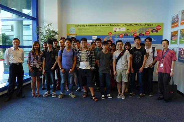
23 final year students from DEEE Microelectronic & Nanotechnology had the opportunity of visiting Systems on Silicon Manufacturing Pte Ltd (SSMC) on 19 November. Located at Pasir Ris Industrial Drive 1, SSMC’s core business SSMC is to produce CMOS wafer fabrication that offer 0.25micron to 0.11micron logic derivatives and embedded flash CMOS manufacturing process.
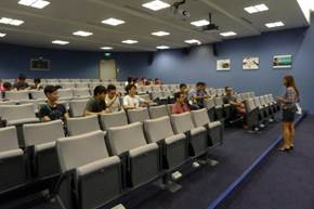
The students were shown a video on the SSMC culture, showcasing their products, job opportunities and benefits that their staff enjoy.
|
A tour of the Fab Lab exposed the students to the real-life working environment in a cleanroom. They observed how engineers, technicians, and operators worked together to handle the various high-tech machines. During the walk-through, our students learnt about the operation of every process station which included etching, deposition, ion implantation, diffusion, photolithography, wafer polishing and testing. They observed the commitment and passion of each individual working on operating the process systems and the testing of wafer chips.
|

|
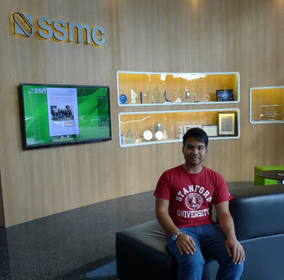
| “I was mesmerised by everything I saw in the Semiconductor Fab facility. It started from the time I walked between large manufacturing machines worth millions of dollars to observing wafers being transported around the Fab by automated systems, and observing hardworking engineers, technicians, and operators performing their tasks. We are very grateful to the friendly manager who guided us around the Fab and answered our questions. The final segment of the visit included a brief overview and roadmap of SSMC and a talk on recruitment. SSMC inspires polytechnic students by allowing us to view the actual working environment, and offering jobs upon graduation. In conclusion, SP and SSMC have shown Nanotechnology students that what we learn here is directly applicable to an industry now worth more than US$200 billion. SP has shown that there is more to learn beyond the classroom and that opportunities are limitless if one is truly interested in his own field of study.” |

Ikhwan from class DEEE3A58 had this to say:
|
The field trip proved fruitful as many students were inspired to either work or further their studies in the semiconductor industry in the future. The visit also widened their knowledge of the semiconductor industry and the working culture in a wafer fabrication environment.
