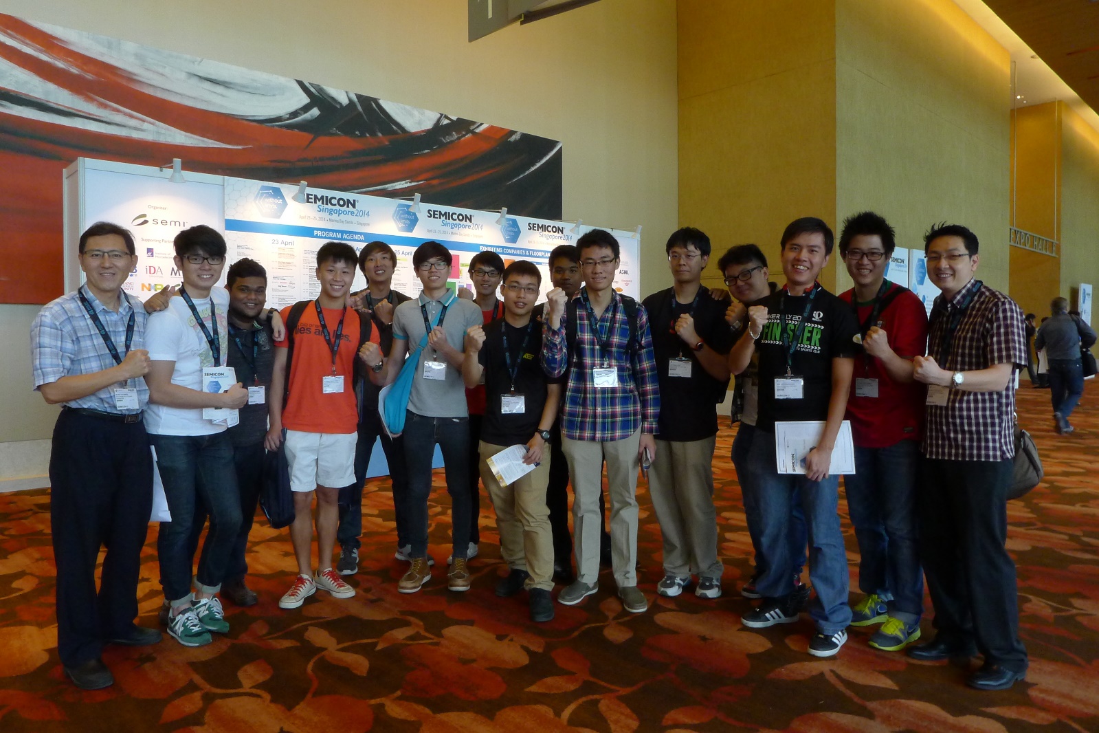
Industry field visit to SEMICON University Program 2014
16 Apr 2014
Our DEEE Micro & Nano students were invited to the SEMICON University Program on 25 April to have an understanding of the key industry players in Singapore. They were also given a short tour on the exhibits from various companies serving the microelectronics and semiconductors industry.
SEMICON University Program 2014, held at Marina Bay Sands Expo and Convention Centre, is a semiconductor event in Southeast Asia that provides a platform for industry leaders, companies, graduates and working professionals to come together.

After a welcome by Mr Ng Kai Fai, President of SEMI Southeast, Mr. Gabriel Lim from Economic Development Board (EDB), talked about the outlook for the semiconductor industry in Singapore. He mentioned there is a strong demand for talents in the IC design industry and are looking at polytechnics and university graduates as well as engineers from Research Institutes to support this. He also added that presently there are a few programs that provide scholarships in IC Design & Semiconductor from EDB.


A technical expert from 3M gave a presentation on “The Future of Touch – Scaling Beyond the Smart Phone: Meeting Touch Expectation in an Expanding Market”.

A tour of the exhibition tour in the TECH Fair saw exhibitors showcasing their products and services to illustrate the various technologies supporting the Semiconductor and IC Design industry. Our students listened attentively to the 3M presentation and were impressed with the 3M Multi-touch Display which uses high performance projected capacitive multi-touch technology, offering an uncompromised touch experience.


The exhibitor from YASKAWA showcased their robotics technology, the development of mechatronic equipment, clean/vacuum robot and wafer handling devices. Our students were captivated by the Dual-arm MOTOMAN Robot that was able to complete a scrambled Rubik’s cube, and were amazed at how smoothly the robot turned the cube and completed the task in less than 40 seconds.


Another exhibitor, NXP showcased smart lighting control through wireless energy harvesting switch and tablet. The wireless energy harvesting switch is a compact alternative to conventional wired switches. The required RF energy is created by the mechanical actuation of the switch, and the data is transmitted wirelessly via RF technology. Another technology they showcased was the Smart Wireless Charging on mobile devices. It enables devices to be charged without the need for cords, connectors or electrical plugs. Wireless charging allows power to be transferred wirelessly from a charging transmitter to a charging receiver.


Finally, the students were brought to view SMART car, a self-driven car which is a collaboration project between NUS & MIT. It is still undergoing testing in a closed-monitored environment. There are plans to test this vehicle on public roads in the middle of the year.


At the end of the program, the students listened to experts from different companies talk about their career in the semiconductor industry -these included Advantest, ASE Singapore, Arrow Technologies, ASML, and Lam Research.
The feedback from our students were positive as they gained more knowledge and understanding about the semiconductor industry and products related to it. Here are some quotes:
-
“Engineers pave the way for the future. The sky is the limit.”
-
“Exhibits were helpful in showing about technology and products in semiconductors industry.”
-
“It gave me a whole new experience in seeing how nanotechnology improve our lives better and more convenient through creation of new products and devices.”
-
“Engineering is a job with a good future and prospects”
