Semiconductor and Electronics Hub
About the Tech hub
This hub is part of the core Technology Hubs under the School of Electrical and Electronic Engineering. It is set up to address the needs of the industry, focusing on developing capability in design and implementing embedded systems technology and semiconductor
process technology.
The hub supports the platform for staff and students with facilities to carry out a wide spectrum of embedded technology and semicon projects.
The hub consists of the following facilities:
- IC Design @ T12201
- Nanofab lab @ T12A203
The Nanofab and IC Design labs were established in 2000. It provides the facilities to train students for the semiconductor industry and technology development in the areas of IC design, embedded solutions (FPGA), Wafer Fabrication, Micro-Electromechanical
Systems (MEMS), Micro/Nanofabrication and Flexible Electronics. The Nanofab lab comprises a 450-square metre cleanroom of class 100 & class 1000 and houses the facilities for fabrication of IC, MEMS, Flexible Electronics and PV cell. The IC Design
lab houses workstations with IC Design software such as Cadence and Xilinx software.
The hub seeks collaboration with industry and academic/research institutes in joint R&D and industry projects involving staff and students to improve competencies in the area of embedded solutions, IC design & nanofabrication.
In addition, they also provide customised courses to retrain and upgrade manpower for electronic and semiconductor industries.
Capabilities and Technical Services
The hub specialises in R&D and applied projects in the following technology areas:
- Electronic Systems Design (FPGA, SoC, IC Design)
- Microfabrication
- Flexible Electronics
This tech hub provides the facilities and have the processing capabilities for Wafer Fabrication, PV cell, MEMS and Flexible Electronics. They also offer consultancy work in embedded solutions, electronic system design and Micro-fabrication.
Project Showcase
Some of the projects in collaboration with IHLs, industry and research institutions are:
Artificial Intelligence and IoT solutions using FPGA
FPGA, or Field Programmable Gate Array is a fully re-configurable integrated chip. FPGA offers high throughput, low latency, low power consumption, and has demonstrated better performance compared to CPU and GPUs. It is valuable at reducing memory
buffering time and defeating I/O bottlenecks, which are important restricting factors in Artificial Intelligence (AI) system performance. In addition, the unique architecture of FPGAs provides the flexibility required to support customizable
applications, making them a generic solution.
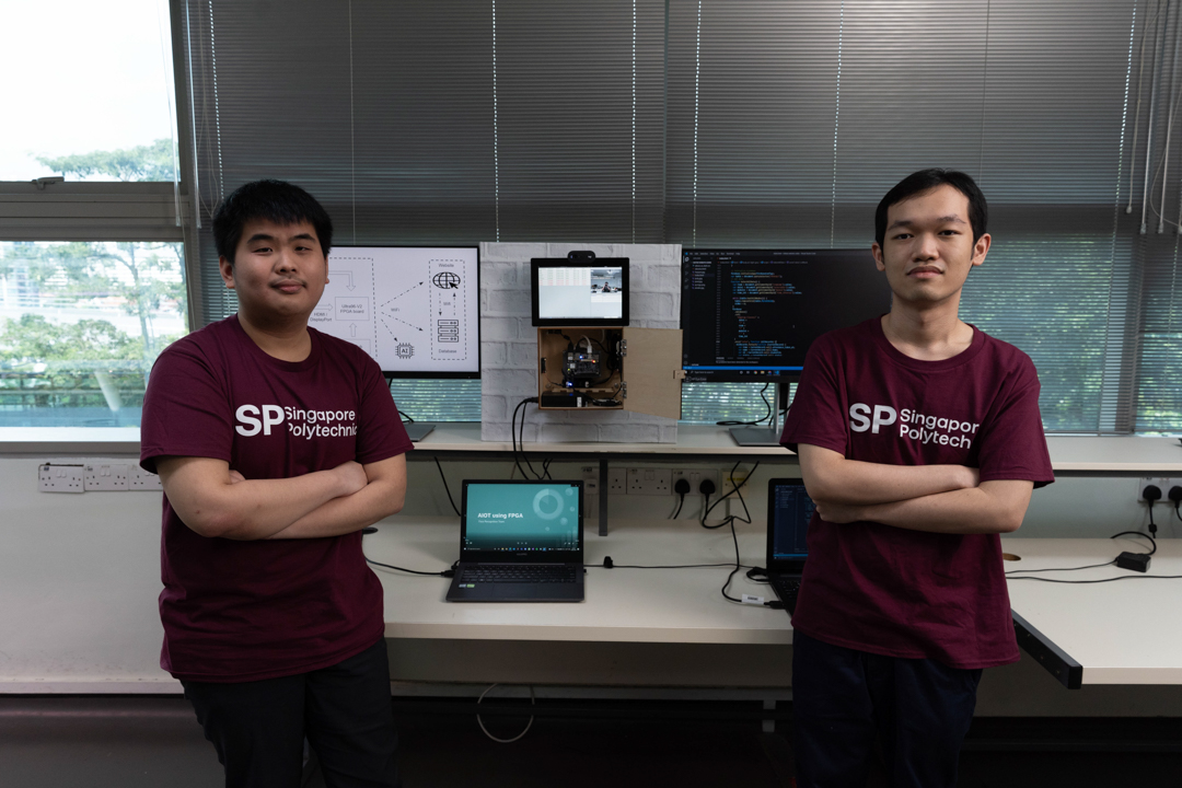
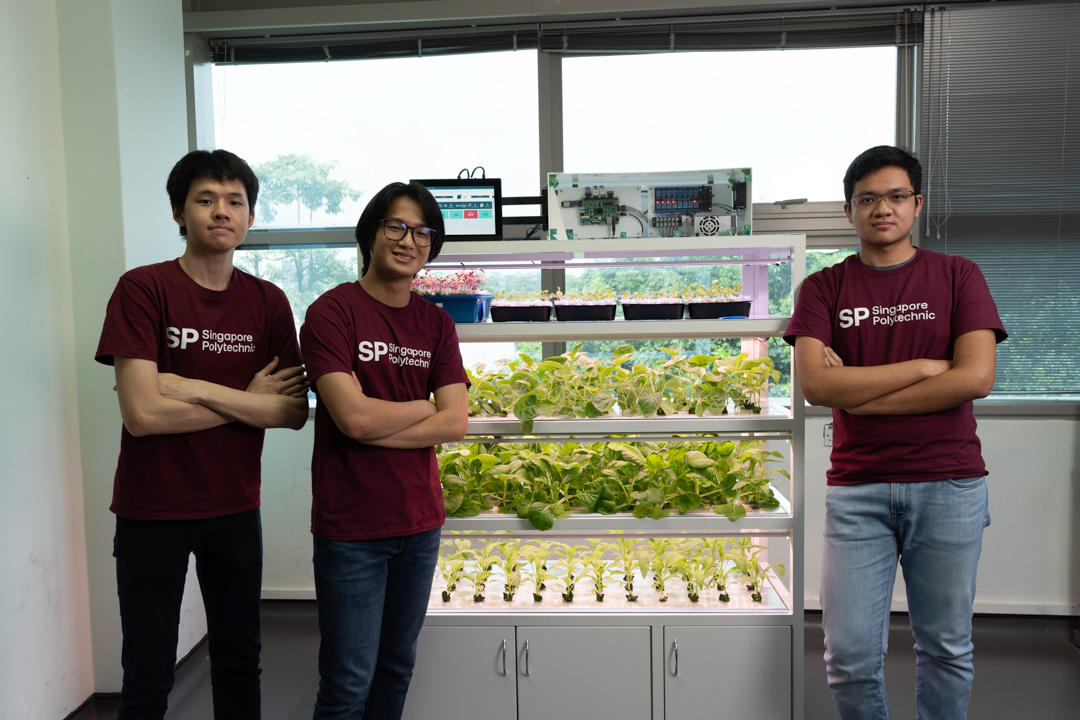
Some of the projects that the techhub has worked on are developing AIoT solutions using FPGA technology such as a face recognition AIoT system for automatic attendance taking and tracking, an AI-enabled IoT-control system for urban farming applications,
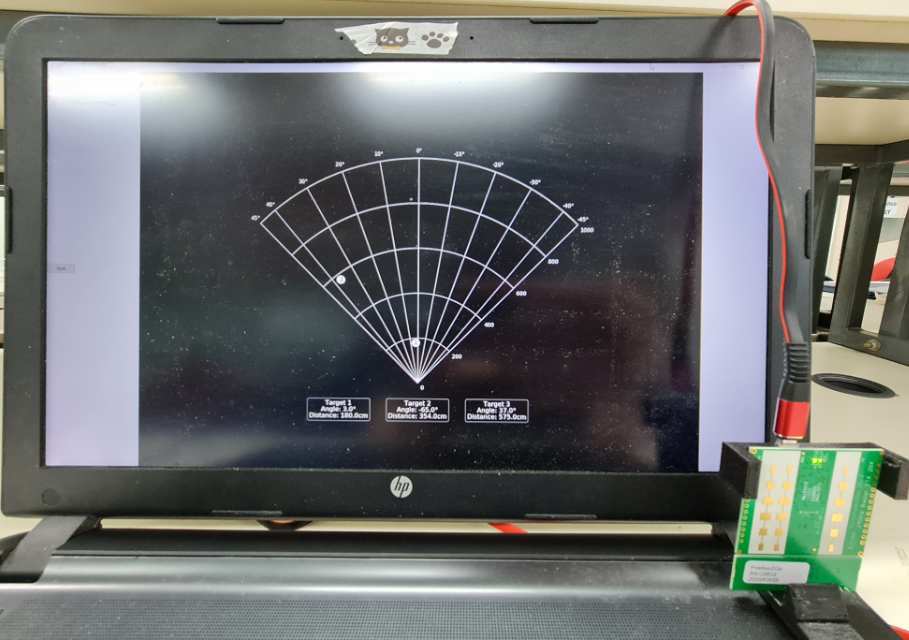
employing radar sensor with FPGA for security applications and a software-defined radio (SDR) driven 4G/5G communication system.

Face recognition AIoT system for automatic attendance taking and tracking

AI-enabled IoT-control system for urban farming applications

Radar sensor with FPGA for security applications
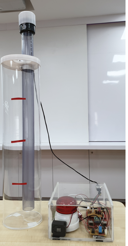
Flood Monitoring System (in collaboration with Infineon Technologies)
This project uses pressure sensor, security chip and microcontroller from Infineon Technologies to develop a flood monitoring system for early warning flood alert.

Flood Monitoring System
Custom IC/FPGA-based design:
- Robotic Soccer Image Processor
- Serial Communication Protocol
- Analog IC : CMOS voltage regulator, filter and operational amplifier
MEMS/Flexible Electronics/Clean Energy(in collaboration with NTU, NUS and DSO):
- Carbon Nanotube (CNT) applications
- PV cell (crystalline silicon and polymer)
- Micro-fuel cell
- Microfluidic applications; micro-grippers, micro-assay chip, micro-optofluidic
- switch/lens, micro-pump, micro-valve, micro-mixer and particle sorters
- Micro-mirror
- Micro-actuators
- Energy Harvester
- Biochips
- Flexible sensors
Biochips
Collaboration
The hub has worked with the following partners:
- Nanyang Technological University (NTU)
- National University of Singapore (NUS)
- Defence Science Organisation (DSO)
- A*Star institutions
- Industries
Courses and seminars
The hub conducts courses and seminars in the following areas:
- Embedded Solutions
- FMEA
- Wafer Fabrication
- Clean room; micro contamination control and management
- Vacuum Technology
- Micro-fabrication processes; photolithography, etching, deposition, etc
- Micro-ElectroMechanical Systems (MEMS)
- IC Design
- IoT for Electronics Industry
- Data Analytics for Electronics Industry
 | Ms Cassandra Low Lee Ngo
Manager, Technology Development
School of Electrical and Electronic Engineering
Email: LOW_Lee_Ngo@sp.edu.sg
Phone: 67721247
Fax: 6772 1974 |